OpenFixture is a fully parametric programming/test fixturing solution written in openscad. The inputs are generated/captured from the users board layout software and a laser cuttable fixture is generated automagically. Enjoy!
Important Links:
Below is a brief introduction to the motivation behind OpenFixture. If you want to jump straight into making one follow these steps:
- Export outline and coordinates from kicad
- Generate laser cuttable DXF using openscad
- Laser cut parts or use a service like ponoko
- Verify BOM
- Assemble
While working on a product I’ve been developing over the last 18 months I iterated through many revisions of the PCB. Sometimes to test new ideas, sometimes to fix issues with earlier revisions. Due to the small form factor of the design and PCB there was no room for a proper JTAG/SWD header. In addition there were other test points that I wanted to bring out to quickly examine signal integrity on the analog front end. In previous revisions I had tried various approaches.
- Fly wire directly to the test points.
- Added a 2×10 Cortex 2mm spaced connector on the non-component side.
- Added 0.1″ spaced single row header along the edge.
All of the above approaches had one glaring issue apart from the extra soldering involved: When it came time to test in the plastics the connector needed to be unsoldered or the wires shielded to avoid shorts when it was stuffed back into the plastics.
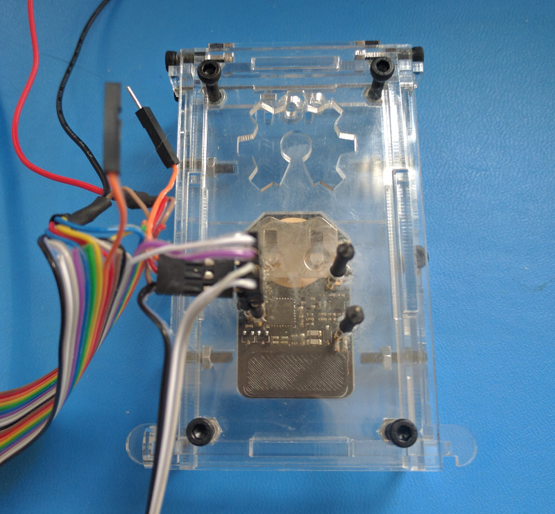
The solution was of course nothing new and common to all commercial PCBs: Add test points as needed in convenient locations and build a test fixture to make contact during programming/debug. Then when testing in the final plastics the PCB assembly can simply be popped out, a battery inserted, and testing can begin.
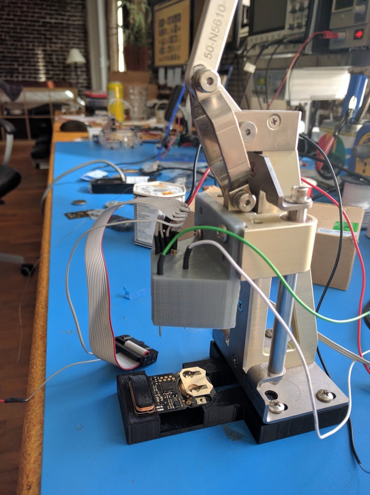 For the fixture I used a vertical sliding assembly that was leftover from a project with a previous employer. I then 3d printed the base to fit the PCB outline along with a head that lined up with the test points. After a couple iterations of moving the test points in the head I was able to get everything to line up and it worked just as expected. I’ve been using this solution from PCB revisions 5-9 and it’s worked well without issues. However, there are a few shortcomings…
- It’s built on a proprietary platform (from previous employer) that cannot be easily reproduced.
- The cost of the metal assembly and pillow blocks would be high were I to reproduce it.
- 3D printing is slow… painfully slow when you have a freshly baked PCB you want to test.
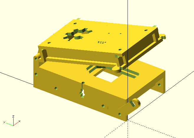
After 3D printing at least 8 heads and a few bases I started to brainstorm a new solution. I actually developed a new solution every morning for 3 days until I was happy. The first was built on a Chebyshev linkage but it had too much slop in it with 4 joints on each side. After that I went to the single hinging mechanism. The problem with that was the test pins are built to be depressed in an orientation 90 degrees to the board. The second iteration didn’t take this into account and contact was made around 88.5 degrees which caused the pins to slip around and not compress smoothly. Using a little trigonometry I set up a constraint of “minimum contact angle” which resized the rest of the geometry. The result was smooth and accurate compression of the test points. This final iteration I dubbed OpenFixture.
OpenFixture takes a few generated outputs from kicad plus a few variables from the user and generates a fully parametric PCB fixture ready to be laser cut at your nearest hackerspace or using a service like ponoko. I mention Kicad above because that is my EDA tool of choose. The same should be possible with Eagle, Altium, etc. Please shoot me an email if anyone has had luck with the other design suites: info@tinylabs.io.